
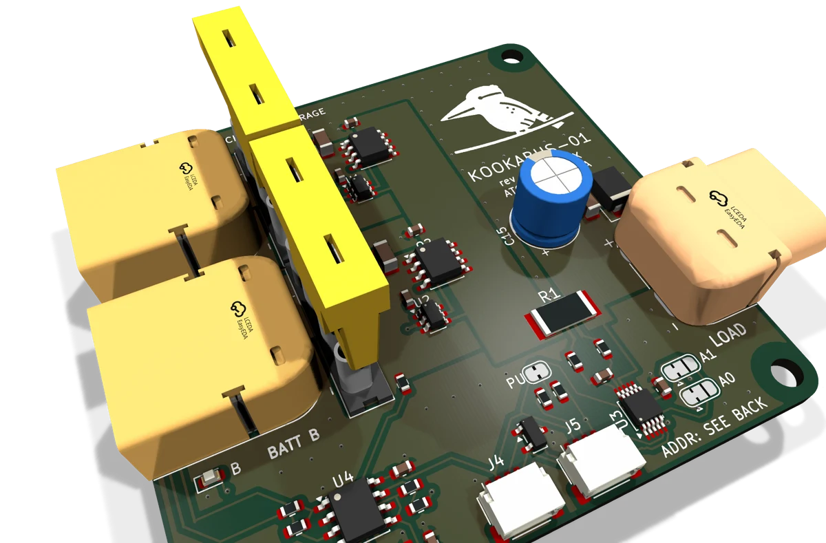
Overview
Kookabus-01 joins two lithium-ion packs into one uninterrupted supply for a robot or other mobile load. Each pack feeds an ideal-diode stage, so the higher-voltage pack carries the load and a pack can be unplugged and replaced while the other keeps the bus up. A high-side current and voltage sensor on the output reports bus voltage, current and power over I²C through two Qwiic/PiicoDev connectors. An LED beside each battery connector shows which pack is supplying the load.
The board is a power pass-through. It does not regulate, charge or balance, and it needs no configuration to swap packs: the ideal diodes run from the packs themselves. The sensor and LEDs draw their 3.3 V from the I²C host.
- Two XT60 battery inputs, one XT60 load output, common ground.
- 5S lithium-ion packs as the primary target. Every part is rated for 6S (25.2 V).
- 100 W peak, 40 W continuous. 6.7 A peak and 2.7 A continuous from a flat 15 V pack.
- Ideal-diode ORing. 20 mV regulated forward drop, no brownout on swap, reverse-current blocking.
- Reverse-polarity tolerant inputs. A reversed pack is blocked, not shorted.
- INA226 high-side monitor. 1.25 mV bus voltage LSB, 0.5 mA current LSB, 16-sample averaging.
- I²C at 3.3 V logic, four selectable addresses with 0x40 default, on-board pull-ups with a cut jumper.
- Two Qwiic/PiicoDev connectors for daisy-chaining, with ESD protection on SDA and SCL.
- One 10 A ATO blade fuse per pack, replaceable without tools.
- Bidirectional 33 V TVS on each input, 26 V TVS on the output.
- Active-pack indicator LEDs, red for A and yellow for B.
- Standby drain about 0.32 mA per pack with the host off.
- 64 × 62 mm, four M3 mounting holes, all SMD parts on the top side.
Applications
- Hot-swappable battery supply for ROS 2 and other mobile robots.
- Battery monitoring for Raspberry Pi, Jetson and microcontroller hosts.
- Bench supplies built from cordless-tool packs: Ryobi ONE+, Einhell Power X-Change and similar 5S packs on XT60 adapter leads.
Board revision 2, datasheet revision 1.0, 25 September 2026. Preliminary: values not marked as measured are from design calculations and component datasheets.
Specifications
Recommended operating conditions. Stay inside these for rated performance. Absolute limits are in the ratings section.
| Parameter | Min | Typ | Max | Unit | Note |
|---|---|---|---|---|---|
| Pack voltage, each input | 12 | 18 | 25.2 | V | 5S primary (15.0 V flat to 21.0 V full). 6S full charge is the maximum. The ideal-diode controllers work from 3.2 V but the sense and LED circuits are meant for 5S to 6S. |
| Pack chemistry | Lithium-ion or LiPo, 5S or 6S. Any chemistry in the voltage range works; the board does not charge or balance. | ||||
| Load current, continuous | 2.7 | 7 | A | 2.7 A is 40 W from a flat 5S pack. 7 A keeps every copper pour under a 10 °C rise (IPC-2221, 1 oz, external). | |
| Load current, peak (10 s) | 6.7 | 10 | A | 6.7 A is 100 W from a flat 5S pack. | |
| Load power from a 5S pack | 40 | 100 | W | Continuous, peak. | |
| 3V3 supply from the host | 3.0 | 3.3 | 3.6 | V | Qwiic/PiicoDev standard. Below 2.7 V the INA226 resets. |
| 3V3 supply current drawn from the host | 2 | 4 | mA | INA226, comparator and one lit LED. | |
| I²C bus speed | 400 | 2500 | kHz | INA226 supports up to 2.94 MHz high-speed mode; 100 or 400 kHz is typical for Qwiic cabling. | |
| Operating ambient temperature | 0 | 25 | 50 | °C | At 100 W the FET rises about 30 °C above ambient in still air. |
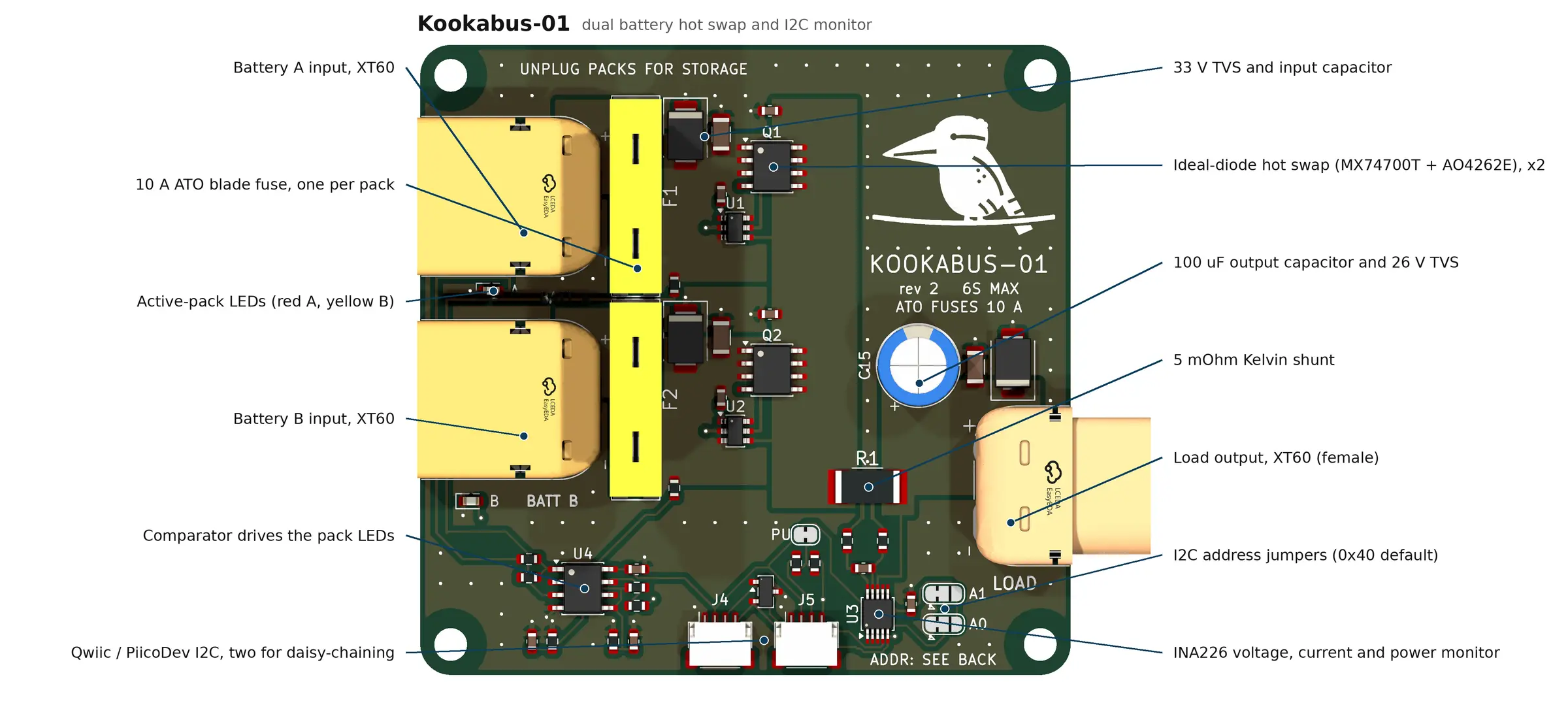
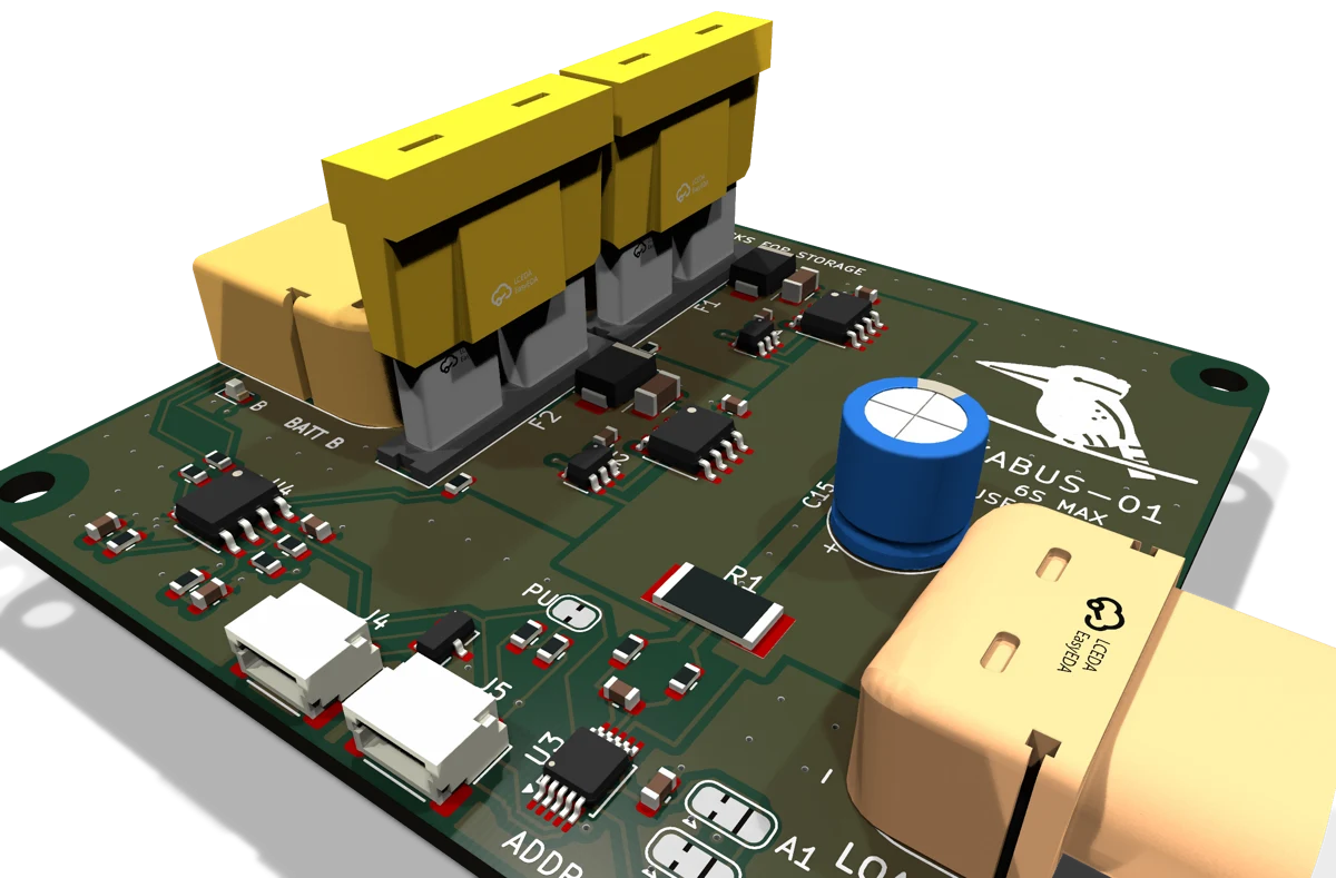
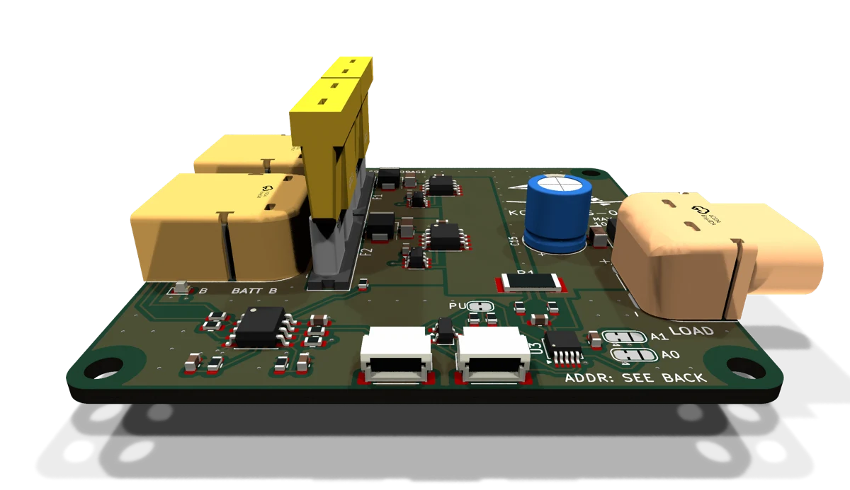
The board
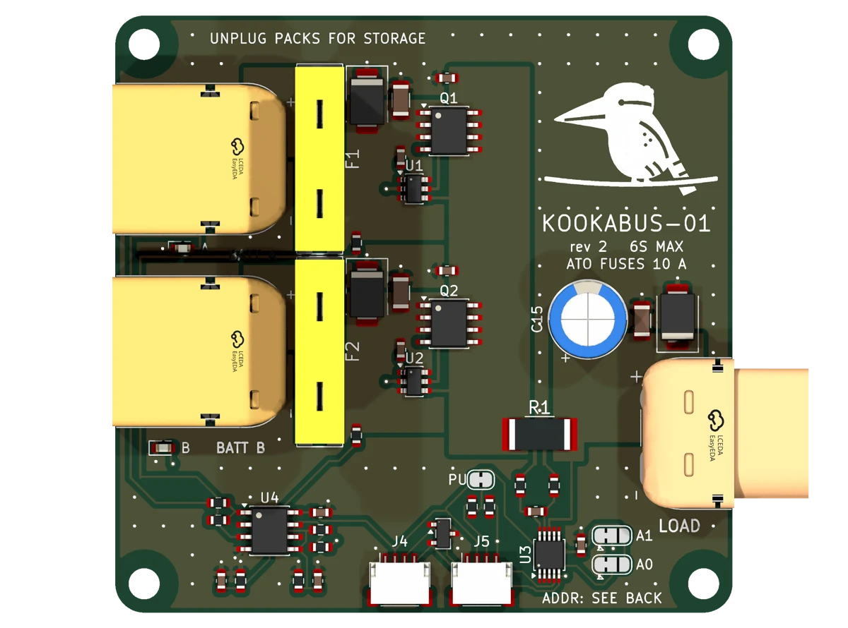
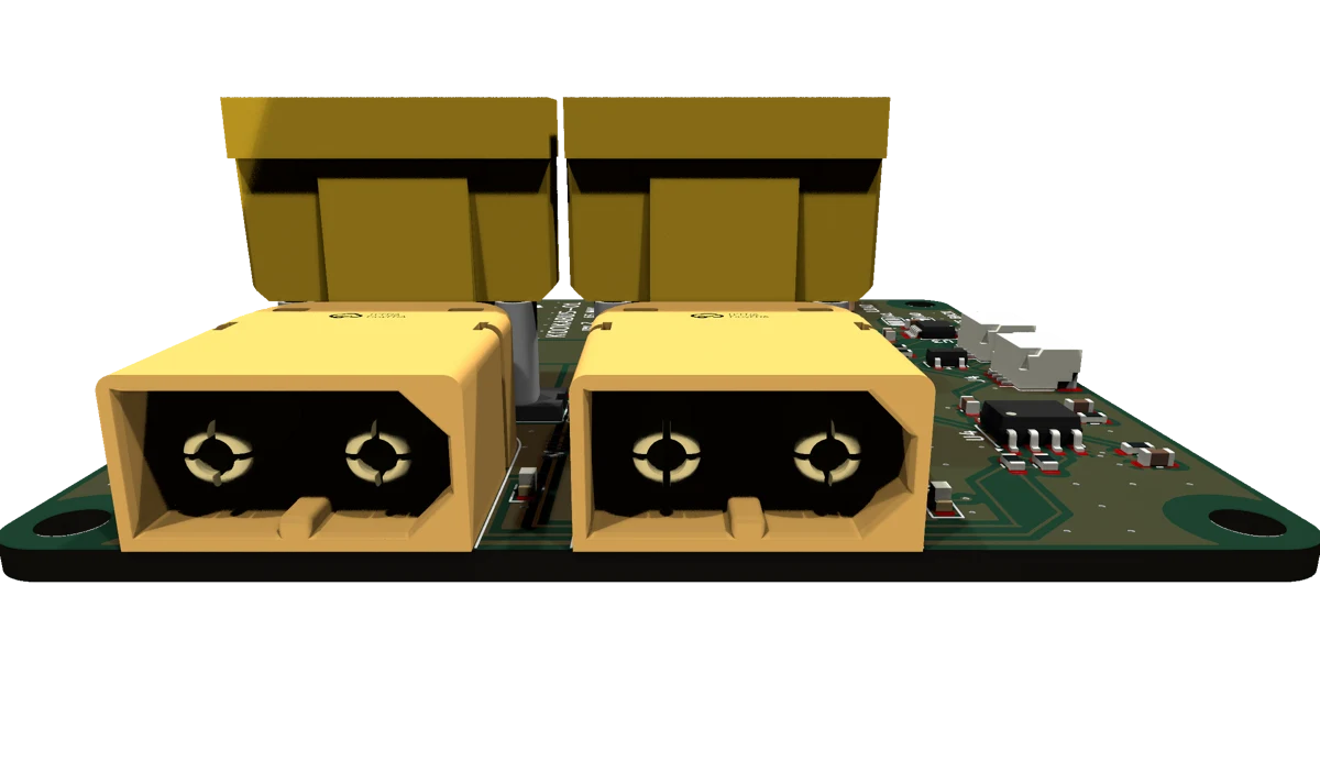
- J1, J2
- BATT A and BATT B. Male XT60 pack inputs.
- J3
- LOAD. Female XT60 output, nose overhangs the right edge.
- F1, F2
- ATO blade fuse holder for each pack. Fit 10 A fuses before use.
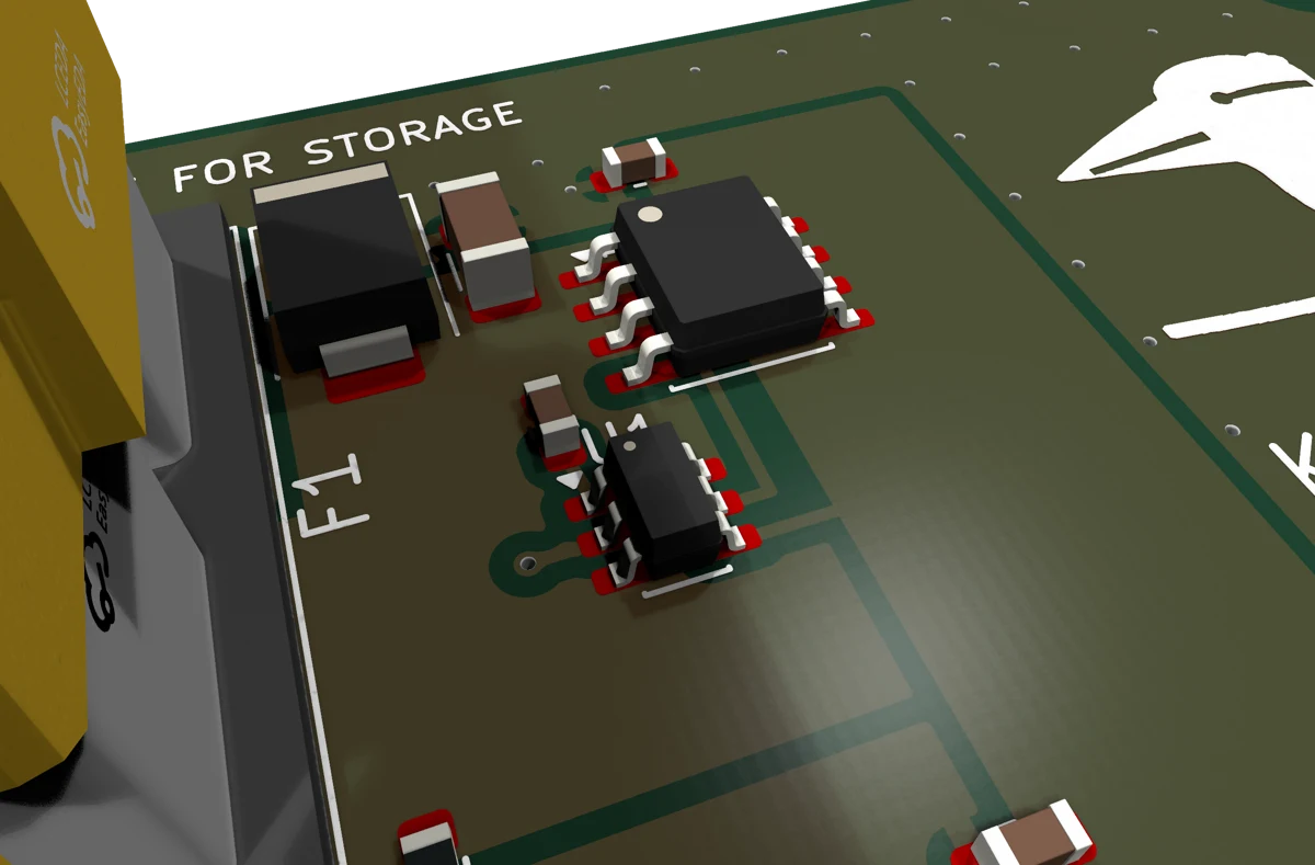
- U1 Q1, U2 Q2
- Ideal-diode stage for each pack: MAX74700T controller and AO4262E 60 V FET.
- C15
- 100 µF output capacitor on VLOAD, in parallel with 4.7 µF ceramic.
- R1
- 5 mΩ 2512 shunt, Kelvin sensed.
- U3
- INA226 voltage, current and power monitor.
- U4
- MCP6002 comparator driving the two active-pack LEDs.
- LED A, LED B
- Red beside BATT A, yellow beside BATT B. The lit one is supplying the load.
- J4, J5
- JST SH 4-way I²C connectors, wired in parallel.
- A0, A1
- JP1 and JP2, INA226 address jumpers.
- PU
- JP3, cut to remove the 4.7 kΩ pull-ups.
More views
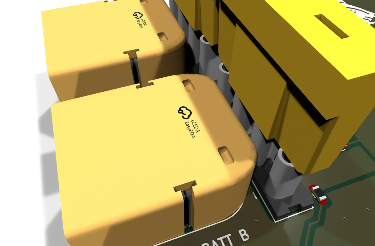
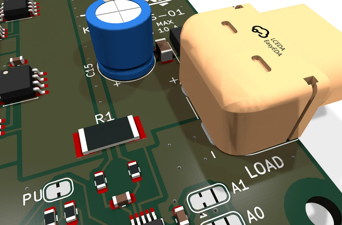
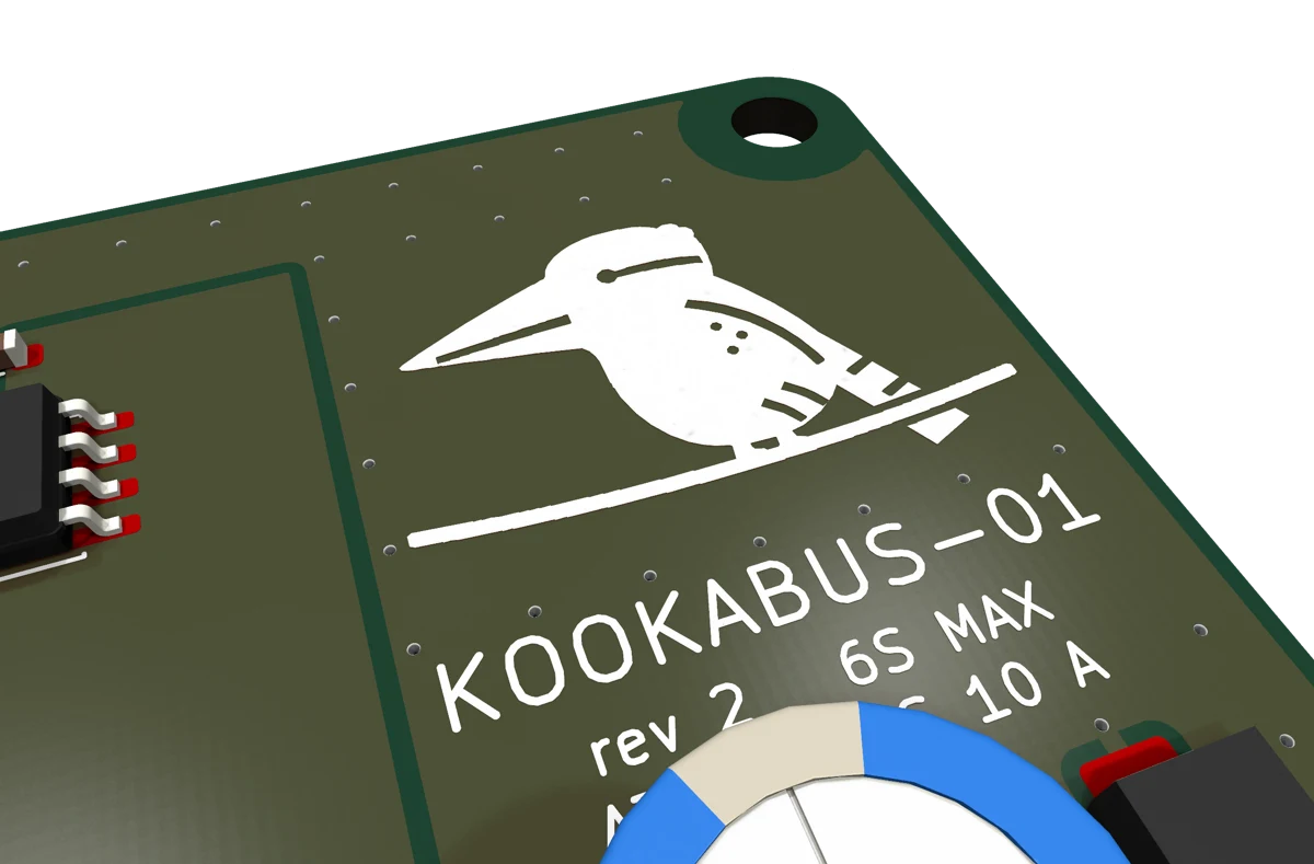
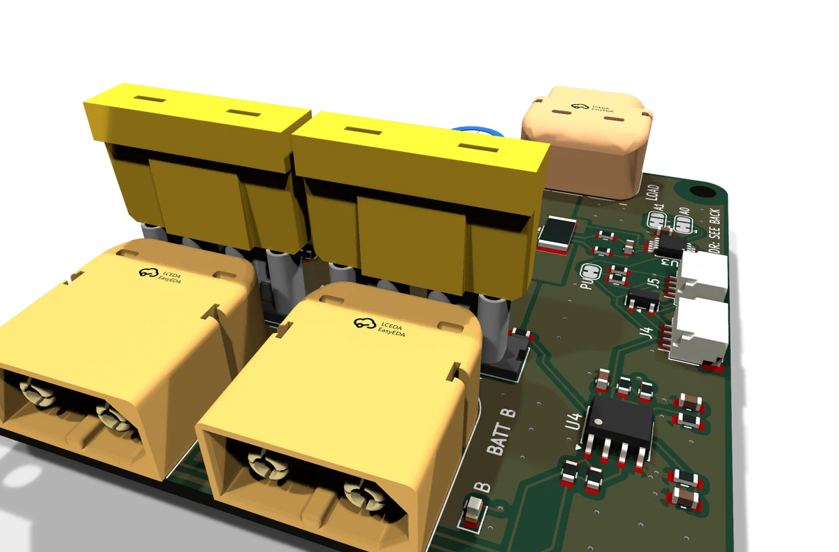
How the hot swap works
Only the pack with the higher voltage conducts. When the two packs are within about 20 mV of each other both stages conduct and share the load. When a pack is unplugged, the other pack's FET body diode conducts immediately and its controller then enhances the FET, so the bus never drops out. Current cannot flow back into a pack: a fully charged pack plugged in beside a flat one does not charge the flat one.
Nothing on the board needs to be told a swap is coming, and the hot swap works with nothing connected to J4 or J5. Only the LEDs and the I²C reading need the host's 3.3 V.
Typical connection
- Fit a 10 A ATO fuse in F1 and F2.
- Connect the robot's power input to LOAD with a male XT60 lead.
- Connect the host's Qwiic or PiicoDev port to J4 with a 4-way JST SH cable. Use J5 to chain further I²C boards.
- Plug the first pack into BATT A. Its LED lights once the host's 3.3 V is present.
- Plug the second pack into BATT B. To swap packs later, unplug the one whose LED is off, replace it, and repeat for the other. The load never loses power as long as one pack stays connected.
Unplug packs for storage. Each pack drains about 0.32 mA while plugged in with the host off, which empties a 5 Ah pack at 10 % charge in about 65 days.
Ratings
Absolute maximum ratings
Stresses beyond these values may cause permanent damage. These are limits, not operating conditions.
| Parameter | Min | Max | Unit | Limiting part or note |
|---|---|---|---|---|
| Battery input voltage, BATT A or BATT B to GND | -26 | 33 | V | SMBJ33CA standoff. Negative: a reversed 6S pack is blocked by the ideal diode (FET VDS 60 V, worst case 50.4 V with a 25.2 V bus). |
| Transient on a battery input (clamped) | 53.3 | V | TVS clamp at its rated 11.3 A surge, microseconds only. | |
| Load output voltage, LOAD to GND | -0.3 | 26 | V | SMBJ26A standoff. Voltage applied to the output from the load side (regen) is absorbed only by the output capacitor and TVS. |
| Load current, continuous | 10 | A | Fuse rating. Above about 8 A the fuse and copper run hot. | |
| 3V3 pin (Qwiic connector) to GND | -0.3 | 5.5 | V | INA226 supply limit. |
| SDA, SCL to GND | -0.3 | 5.5 | V | PESD5V0S2BT clamps ESD; INA226 and pull-up rail set the DC limit. |
| ESD on SDA, SCL (IEC 61000-4-2, contact) | 8 | kV | PESD5V0S2BT. | |
| Operating ambient temperature | -20 | 70 | °C | Limited by the electrolytic output capacitor and connectors. Not characterised over temperature. |
| Storage temperature | -40 | 85 | °C | Packs unplugged. |
Electrical characteristics
Calculated at 25 °C from component datasheets unless stated. VBUS is the ORed node after the ideal diodes; VLOAD is the load connector after the shunt.
Power path
| Parameter | Condition | Min | Typ | Max | Unit |
|---|---|---|---|---|---|
| Ideal-diode regulated forward drop (BATT to VBUS) | Load below about 3 A | 13 | 20 | 29 | mV |
| FET on-resistance (per stage) | VGS about 12 V, 25 °C / 125 °C junction | 6.5 / 10.5 | mΩ | ||
| Total input to output drop, fuse to LOAD | 2.7 A (40 W) | 70 | mV | ||
| 6.7 A (100 W), FET hot | 190 | mV | |||
| Series resistance, fuse to LOAD (excluding the regulated drop) | Fuse 7.7 mΩ, FET, shunt 5 mΩ, copper, connectors | 30 | mΩ | ||
| Board dissipation | 2.7 A / 6.7 A | 0.18 / 1.25 | W | ||
| Pack sharing window | Both stages conduct when packs are within | 20 | mV | ||
| Reverse current, VBUS into a pack | Lower pack, or pack removed | 0 | A | ||
| Time to enhance the FET on first connection | Body diode carries the load until then | 2.3 | ms | ||
| Ideal-diode controller supply current, per pack | Always, from the pack | 300 | µA | ||
| Standby drain per pack, host off | Controller plus pack-voltage divider | 0.32 | mA | ||
| Output capacitance on VLOAD | 100 µF electrolytic plus 4.7 µF ceramic | 105 | µF | ||
| Input capacitance, each pack | 4.7 µF 50 V ceramic | 4.7 | µF |
Monitor (INA226, U3)
| Parameter | Condition | Min | Typ | Max | Unit |
|---|---|---|---|---|---|
| Bus voltage measurement point | VLOAD, the load side of the shunt | 0 | 36 | V | |
| Bus voltage LSB | Register 0x02 | 1.25 | mV | ||
| Bus voltage error relative to the live pack | Series drop at 40 W / 100 W; add back I × 0.03 Ω if wanted | -0.07 / -0.19 | V | ||
| Shunt resistance | 2512 alloy, 3 W, 50 ppm/°C, Kelvin sensed | 5 | mΩ, 1 % | ||
| Shunt voltage LSB | Register 0x01 | 2.5 | µV | ||
| Current full scale | 81.92 mV / 5 mΩ | ±16.4 | A | ||
| Current LSB | CALIBRATION = 2048 | 0.5 | mA | ||
| Current offset | INA226 10 µV input offset | 2 | mA | ||
| Current gain error | Shunt tolerance plus INA226 0.1 % | 1.1 | % | ||
| Power LSB | 25 × current LSB | 12.5 | mW | ||
| Conversion time, bus and shunt | Default 1.1 ms each, 1 sample | 0.14 | 1.1 | 8.2 | ms |
| Sense input filter | 10 Ω series, 100 nF differential | 80 | kHz |
Indicators and I²C
| Parameter | Condition | Typ | Unit |
|---|---|---|---|
| LED A (red) lit | Pack A voltage above pack B, host 3.3 V present | ||
| LED B (yellow) lit | Pack B voltage above pack A, host 3.3 V present | ||
| Indicator hysteresis | Other pack must be higher by this amount before the LED changes over | 0.33 | V |
| Indicator channel mismatch | 1 % dividers; either LED may light when packs are closer than this | 0.2 (0.8 max) | V |
| LED current | 1 kΩ from 3.3 V | 1.4 | mA |
| I²C pull-up, SDA and SCL | To 3V3 through jumper JP3 (fitted, bridged) | 4.7 | kΩ |
| I²C address | JP1 and JP2 as supplied | 0x40 |
Connectors and jumpers
Power connectors
| Ref | Label | Part | Pin 1 | Pin 2 | Note |
|---|---|---|---|---|---|
| J1 | BATT A | Amass XT60PW-M (male, PCB) | GND | + (PACK_A) | Mates with a female XT60 pack lead. Polarity is marked on the silkscreen. |
| J2 | BATT B | Amass XT60PW-M (male, PCB) | GND | + (PACK_B) | As J1. |
| J3 | LOAD | Amass XT60PW-F (female, PCB) | GND | + (VLOAD) | Female so a pack lead cannot be plugged into the output. Its nose extends 7.8 mm past the board edge so the load plug's shroud slides over it. |
All three connectors share one ground. There is no isolation between the packs, the load and the I²C host.
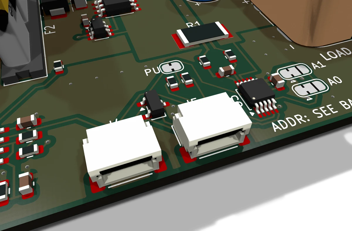
I²C connectors
| Ref | Part | Pin 1 | Pin 2 | Pin 3 | Pin 4 |
|---|---|---|---|---|---|
| J4, J5 | JST SH 1.0 mm 4-way horizontal (SM04B-SRSS-TB compatible) | GND | 3V3 (in) | SDA | SCL |
The pin order is the Qwiic and PiicoDev standard, so any Qwiic cable connects directly. J4 and J5 are wired in parallel for daisy-chaining. The host must supply 3.3 V on pin 2: the board has no regulator of its own, and the monitor, comparator and LEDs stay off until it does. The hot-swap function does not depend on the host.
Solder jumpers
| Ref | Silkscreen | Function | As supplied |
|---|---|---|---|
| JP1 | A0 | INA226 address pin A0: three pads, centre to GND side or VS (3V3) side | GND side bridged |
| JP2 | A1 | INA226 address pin A1: three pads, centre to GND side or VS side | GND side bridged |
| JP3 | PU | Connects the 4.7 kΩ SDA and SCL pull-ups to 3V3. Cut the trace between the pads to remove the pull-ups when the host or another board already provides them. | Bridged (pull-ups on) |
I²C address selection
| JP2 (A1) | JP1 (A0) | Address (7-bit) |
|---|---|---|
| GND | GND | 0x40 (default) |
| GND | VS | 0x41 |
| VS | GND | 0x44 |
| VS | VS | 0x45 |
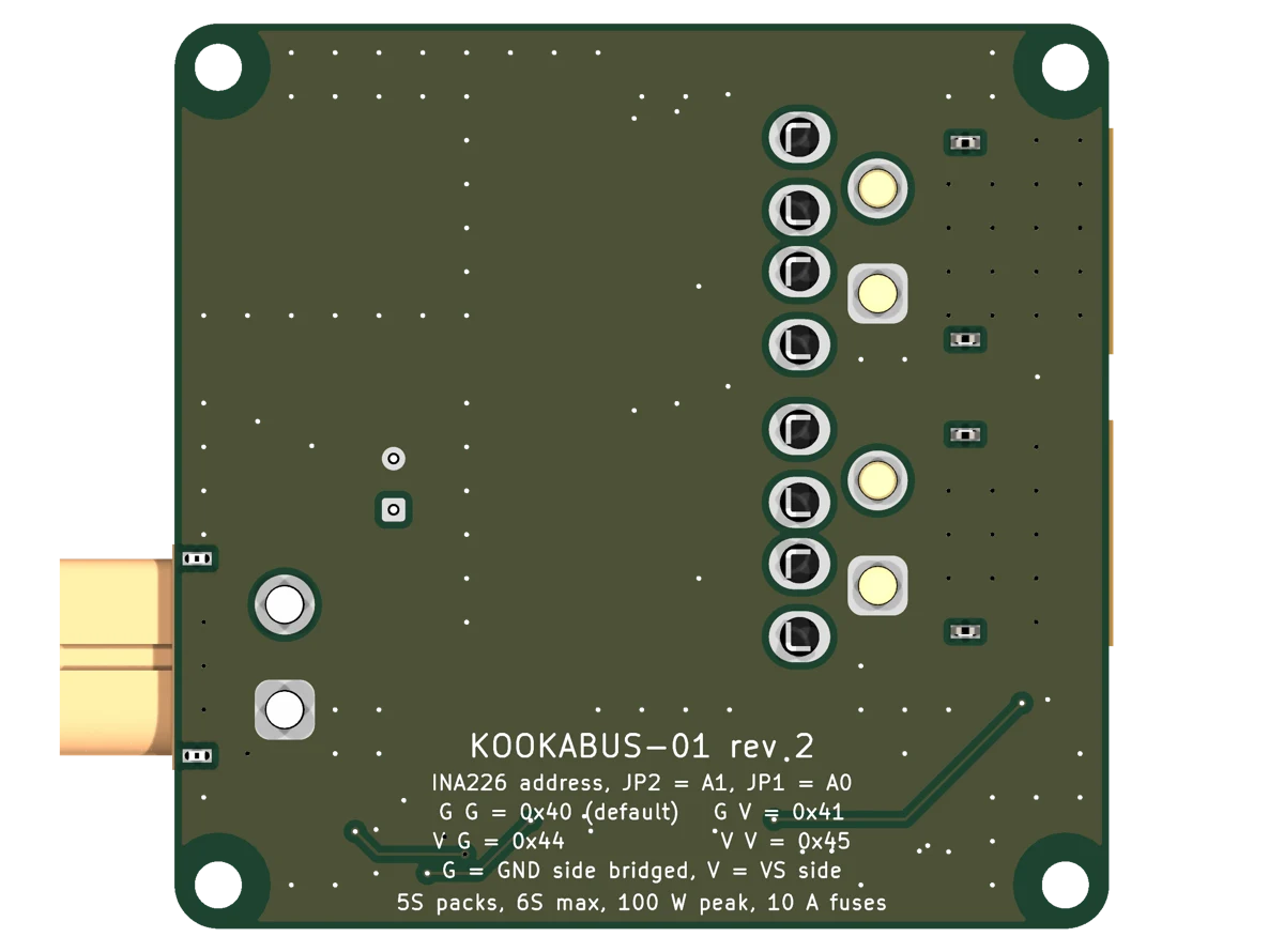
To change an address, cut the bridged trace on the GND side of the jumper, then bridge the centre pad to the VS side with solder. The table is also printed on the back of the board. Up to four Kookabus-01 boards can share one I²C bus.
Fuses
F1 (pack A) and F2 (pack B) are ATO/ATC blade fuse holders rated 30 A at 60 V. Fit a 10 A, 32 V ATO blade fuse in each (Littelfuse 0287010.PXCN or any equivalent). The fuses ship separately and must be fitted before use. A fuse on each pack, rather than one on the output, also protects against a short in that pack's input TVS, capacitor or FET. Blade fuses break more than 1 kA at 32 V, which a tool pack can deliver into a short.
I²C interface
The only I²C device on the board is the Texas Instruments INA226. Its register map applies unchanged; the values below are specific to this board's 5 mΩ shunt. Registers are 16 bits, most significant byte first.
| Address | Register | Use on Kookabus-01 |
|---|---|---|
| 0x00 | Configuration | Reset value 0x4127 (1 sample, 1.1 ms conversions, continuous). Write 0x4527 for 16 sample averaging, which steadies readings with a motor load. |
| 0x01 | Shunt voltage | Signed, 2.5 µV per LSB. Current in amps = value × 2.5e-6 / 0.005. |
| 0x02 | Bus voltage | Unsigned, 1.25 mV per LSB. Valid straight after power-up with no configuration. |
| 0x03 | Power | Unsigned, 12.5 mW per LSB once CALIBRATION is written. |
| 0x04 | Current | Signed, 0.5 mA per LSB once CALIBRATION is written. Positive is current into the load. |
| 0x05 | Calibration | Write 2048 (0x0800) after every power-up of the host 3.3 V. Formula: 0.00512 / (0.0005 A × 0.005 Ω). |
| 0x06, 0x07 | Mask/Enable, Alert limit | Usable, but the ALERT pin is not brought out. |
| 0xFE, 0xFF | Manufacturer ID, Die ID | Read 0x5449 and 0x2260 to confirm the device is present. |
The INA226 loses its configuration whenever the host's 3.3 V is removed. Write CALIBRATION (and CONFIG if changed) in the host's start-up code, not once at commissioning.
Examples
from smbus2 import SMBus

ADDR = 0x40
with SMBus(1) as bus:
    def rd(reg):
        b = bus.read_i2c_block_data(ADDR, reg, 2)
        return (b[0] << 8) | b[1]
    def wr(reg, val):
        bus.write_i2c_block_data(ADDR, reg, [val >> 8, val & 0xFF])

    assert rd(0xFE) == 0x5449          # INA226 present
    wr(0x00, 0x4527)                   # 16 sample average, continuous
    wr(0x05, 2048)                     # 0.5 mA per LSB with the 5 mOhm shunt
    volts = rd(0x02) * 1.25e-3
    raw = rd(0x04)
    amps = (raw - 65536 if raw > 32767 else raw) * 0.5e-3
    watts = rd(0x03) * 12.5e-3
    print(f"{volts:.2f} V  {amps:.3f} A  {watts:.2f} W")
from machine import I2C, Pin
ADDR = 0x40
i2c = I2C(0, sda=Pin(8), scl=Pin(9), freq=400_000) # Pico pins on a PiicoDev adapter
def rd(reg):
b = i2c.readfrom_mem(ADDR, reg, 2)
return (b[0] << 8) | b[1]
def wr(reg, val):
i2c.writeto_mem(ADDR, reg, bytes([val >> 8, val & 0xFF]))
assert rd(0xFE) == 0x5449
wr(0x00, 0x4527)
wr(0x05, 2048)
volts = rd(0x02) * 1.25e-3
raw = rd(0x04)
amps = (raw - 65536 if raw > 32767 else raw) * 0.5e-3
watts = rd(0x03) * 12.5e-3
print(volts, "V", amps, "A", watts, "W")#include <Wire.h>
const uint8_t ADDR = 0x40;
uint16_t rd(uint8_t reg) {
Wire.beginTransmission(ADDR); Wire.write(reg); Wire.endTransmission(false);
Wire.requestFrom(ADDR, (uint8_t)2);
uint16_t v = Wire.read() << 8; return v | Wire.read();
}
void wr(uint8_t reg, uint16_t val) {
Wire.beginTransmission(ADDR); Wire.write(reg);
Wire.write(val >> 8); Wire.write(val & 0xFF); Wire.endTransmission();
}
void setup() {
Wire.begin(); Serial.begin(115200);
wr(0x00, 0x4527); // 16 sample average, continuous
wr(0x05, 2048); // 0.5 mA per LSB
}
void loop() {
float volts = rd(0x02) * 1.25e-3;
float amps = (int16_t)rd(0x04) * 0.5e-3;
float watts = rd(0x03) * 12.5e-3;
Serial.print(volts); Serial.print(" V ");
Serial.print(amps, 3); Serial.print(" A ");
Serial.print(watts); Serial.println(" W");
delay(500);
}On Linux the kernel ina2xx hwmon driver also supports the part. Declare it in the device tree with compatible = "ti,ina226" and shunt-resistor = <5000> (micro-ohms), and read voltage, current and power from sysfs.
State of charge
The bus voltage reads the live pack minus the series drop. For a percentage estimate, divide by the cell count and use a per-cell resting-voltage table rather than a straight line from 3.0 V to 4.2 V. Under load, correct for sag with the measured current and an estimate of pack resistance, which can be taken from the voltage step when the load changes. Integrating the current register gives a coulomb count for the pack that is currently supplying the load; the board cannot tell the host which pack that is, other than by the voltage reading itself.
Protection and safety
| Event | Response |
|---|---|
| Pack unplugged under load | The other pack takes over with no interruption. The remaining pack's FET body diode conducts within nanoseconds; the controller then enhances the FET. |
| Pack plugged in reversed | Blocked. The ideal-diode FET stays off (VDS up to 50.4 V with a 6S bus, rated 60 V) and the bidirectional input TVS is off at -25.2 V. No current flows and nothing is damaged. |
| Lower-voltage pack connected beside a higher one | No current flows into the lower pack. It takes over when the higher pack discharges to within 20 mV of it. |
| Short on the load or a failed part on the board | The 10 A fuse of the conducting pack opens. Replace it with the same rating. |
| Voltage transient on an input (lead inductance, motor noise) | Clamped by the 33 V bidirectional TVS below the FET and controller limits. |
| Voltage rise on the output (regenerative braking) | The ideal diodes block current back into the packs, so only the 100 µF output capacitor and the 26 V TVS absorb it. Run motor controllers with regenerative braking disabled, or fit a brake resistor. |
| Pack over-discharge | Not protected on the board. The FET body diode always conducts, so the board cannot disconnect a pack. The host must stop the load at the pack's minimum voltage, or the pack must have its own cut-off. |
| Over-current below the fuse rating | Not protected. Currents between 7 A and 10 A are allowed briefly but heat the fuse, FET and copper. |
Warning. Lithium-ion packs can deliver hundreds of amps into a short circuit. Fit the fuses before connecting a pack, keep loose metal away from the XT60 pins, and never bridge the two battery inputs. The board does not charge, balance or disconnect packs. Unplug packs for storage.
Mechanical
| Board size | 64.0 × 62.0 mm, 3 mm corner radius |
|---|---|
| Thickness | 1.6 mm FR-4, 2 layers, 1 oz copper both sides |
| Finish | Lead-free HASL, green solder mask, white silkscreen |
| Mounting holes | 4 × 3.2 mm for M3, centres 3.0 mm from each edge (58.0 × 56.0 mm pattern), isolated from copper, 3.6 mm radius clear for screw heads |
| Component height, top | About 20 mm at the ATO fuses, 13 mm at the electrolytic capacitor, 8.5 mm at the XT60s |
| Component height, bottom | None. Through-hole leads protrude up to 1.5 mm. |
| Connector overhang | BATT A and BATT B: 0.5 mm past the left edge. LOAD: 7.8 mm past the right edge. An enclosure needs cut-outs at both edges. |
| Mass | About 25 g with fuses (estimate) |
Connector positions
Board-local coordinates, origin at the top-left corner of the outline as viewed from the top, x to the right, y down.
| Ref | Centre x (mm) | Centre y (mm) | Note |
|---|---|---|---|
| J1 BATT A | 15.85 | 18.5 | Pins on 7.2 mm pitch along y; face at the left edge |
| J2 BATT B | 15.85 | 38.5 | As J1, 20 mm below |
| J3 LOAD | 56.45 | 47.0 | Pins on 7.2 mm pitch along y; face at the right edge |
| J4 Qwiic | 29.5 | 58.6 | Opening at the bottom edge |
| J5 Qwiic | 38.0 | 58.6 | Opening at the bottom edge |
| F1, F2 fuses | 21.2 | 14.9, 34.9 | Blade slots along y |
| H1 to H4 holes | 3.0, 61.0 | 3.0, 59.0 | 3.2 mm |
Application notes
Host firmware checklist
- Write CALIBRATION = 2048 at every start-up, and CONFIG = 0x4527 if averaging is wanted.
- Poll bus voltage and current at a few hertz. Stop the load, or warn, when bus voltage falls to the pack's minimum (about 15 V for a 5S pack, 3.0 V per cell).
- Detect a swap as a step in bus voltage. The higher-voltage pack always carries the load, so the voltage reading always describes the pack in use.
- Disable regenerative braking in the motor controllers, or fit a brake resistor on the load side.
Using the board without a host
The hot swap works with nothing connected to J4 or J5. Only the LEDs and the I²C reading need the host's 3.3 V. For a bench check, any Qwiic host or a 3.3 V supply on pin 2 of J4 lights the LED of the conducting pack.
Thermal
At 40 W continuous the board dissipates about 0.18 W and barely warms. At the 100 W peak the pass FET of the conducting pack dissipates up to 0.47 W and rises about 30 °C above ambient in still air; the fuse and shunt each add about 0.3 W. No heatsink is required for the rated duty. Sustained operation above 7 A is outside the rating.
Ordering and files
| Product | Kookabus-01, board revision 2 |
|---|---|
| Supplied as | Assembled board without fuses, or bare PCB with the design files |
| Fuses required | 2 × ATO/ATC 10 A 32 V blade fuse |
| Design files | KiCad 10 project, Gerbers, drill, position and BOM files, JLCPCB assembly BOM and placement files |
| Key components | 2 × MX74700T ideal-diode controller (TI LM74700-Q1 compatible), 2 × AO4262E 60 V FET, INA226AIDGSR monitor, 5 mΩ 2512 shunt, MCP6002 comparator, SMBJ33CA and SMBJ26A TVS, PESD5V0S2BT ESD, XT60PW connectors, XF-507P fuse holders |
Revisions
| Board rev | Date | Change |
|---|---|---|
| 1 | 24 September 2026 | First design: 30 A continuous, INA228, on-board 3.3 V regulator, 2 oz copper. |
| 2 | 25 September 2026 | Re-rated to 100 W peak and 40 W continuous for low cost and hand assembly. INA226, MX74700T, AO4262E, 5 mΩ shunt, 10 A blade fuses, no on-board regulator (3.3 V from the host), 1 oz copper, 64 × 62 mm. Named Kookabus-01. |
| Document rev | Date | Change |
|---|---|---|
| 1.0 | 25 September 2026 | First release, for board revision 2. Preliminary: calculated values, not yet measured on hardware. |
Information on this page is believed to be accurate at the date of publication but is provided without warranty. Values marked as calculated have not been verified by measurement. Adventures in Silicon Pty Ltd accepts no liability for damage or injury arising from the use of this product, which connects to lithium-ion batteries capable of high fault currents. The user is responsible for fusing, pack protection, enclosure and compliance with local regulations. Product names are trademarks of their respective owners.